Next, a chemical etching process removes the unwanted copper, leaving only the desired copper traces. To ensure durability and conductivity, a solder mask is applied to protect the exposed copper and define solderable areas. This step also gives the turnkey pcb assembly its characteristic green color.
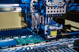
Through-hole plating and surface mount technology are then employed to add electronic components to the board. Holes are drilled where necessary, and components are soldered into place. This process requires precision and care to ensure that the connections are secure and that the components function as intended.
The final step is the application of a silkscreen layer, which adds markings, labels, and other identifiers to help technicians and assemblers during the manufacturing and maintenance stages. The result is a compact and reliable PCB ready to be integrated into a wide range of electronic devices.
Materials and Technologies
PCB fabrication has come a long way since its inception. Modern PCBs are constructed using a variety of materials, including FR-4 (a flame-retardant epoxy-based laminate), metal core substrates, and flexible materials like polyimide, depending on the application. Additionally, advancements in technology have enabled the creation of multi-layer PCBs, which stack multiple circuit layers on top of each other. This allows for more complex and compact designs while maintaining reliability.
Today’s PCBs also incorporate advanced features like controlled impedance, which is crucial for high-frequency applications such as in smartphones and wireless communication devices. This technology ensures that electrical signals can be transmitted accurately and without interference.